01 11

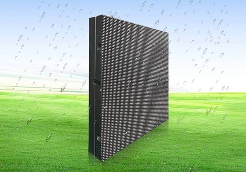
What is the difference between SMD and COB technology and how can I tell the difference?

Introduction

With the rapid development of the commercial display industry in recent years, LED displays are an indispensable part of it, and their technological innovation is changing with each passing day. Among many technologies, SMD (Surface Mount Device) packaging technology and COB (Chip on Board) packaging technology are particularly noteworthy. Today, we will explain the differences between these two technologies in a simple way and show you their respective charms.

SMD and COB LED package technology

SMD (Surface Mount Device) Packaging

First, let’s start with technology. SMD packaging technology is a form of packaging electronic components. SMD, the full name of Surface Mounted Device, means surface mount device. It is a technology widely used in the electronics manufacturing industry to package integrated circuit chips or other electronic components for direct mounting on the surface of a PCB (printed circuit board).

SMD LED package technology

Main features of SMD Packaging:

Small size

SMD-packaged components are small in size, allowing high-density integration, which is conducive to the design of miniaturized and lightweight electronic products.

Lightweight

Since SMD package components do not require pins, the overall structure is lightweight and suitable for applications requiring light weight.

Good high-frequency characteristics

The short pins and short connection paths of SMD packaged components help to reduce inductance and resistance and improve high-frequency performance.

Easy to automate production

SMD packaging components are suitable for the production of automated placing machines, improving production efficiency and quality stability.

Good thermal performance

SMD package components are in direct contact with the PCB surface, which is conducive to heat dissipation and enhances the thermal performance of components.

Easy to repair and maintain

The surface mount of SMD package components makes it easier to repair and replace components.

Package Types

There are various types of SMD packages, including SOIC, QFN, BGA, LGA, etc. Each package type has its own specific advantages and application scenarios.

Technology Development

Since its introduction, SMD packaging technology has developed into one of the mainstream packaging technologies in the electronics manufacturing industry. With the advancement of technology and market demand, SMD packaging technology is also evolving to meet the needs of higher performance, smaller size, and lower cost.

COB (Chip on Board) Packaging

COB packaging technology, the full name of Chip on Board, is a kind of packaging technology that sells the chip directly to the PCB (Printed Circuit Board). This technology is mainly used to solve the problem of LED heat dissipation and realize the tight integration of the chip and circuit board.

COB LED package technology
COB package technology

Technical principle

COB packaging is to attach the bare chip to the interconnect substrate with conductive or non-conductive glue, and then perform wire bonding to achieve its electrical connection. During the packaging process, if the bare chip is directly exposed to the air, it is vulnerable to pollution or man-made damage, so the chip and bonding leads are usually wrapped with glue to form a so-called “soft package”.

Compact packaging

By combining the packaging and PCB, the chip size can be greatly reduced, the degree of integration can be improved, and the circuit design can be optimized to reduce circuit complexity and improve system stability.

Good stability

The chip is soldered directly to the PCB, so it has good vibration and impact resistance. It can also maintain stability in harsh environments such as high temperature and humidity, prolonging product life.

Good thermal conductivity

Using a thermally conductive adhesive between the chip and the PCB can effectively improve the heat dissipation effect, reduce the impact of heat on the chip, and improve the service life of the chip.

Low manufacturing cost

no pins are required, eliminating some complex connectors and pins processes in the manufacturing process, reducing preparation costs. At the same time, automated production can be realized, reducing labor costs and improving manufacturing efficiency.

Notes:

Maintenance difficulties

Due to the direct sale of the chip and PCB, it is impossible to disassemble or replace the chip separately, generally requiring the replacement of the entire PCB, which increases the cost and difficulty of maintenance.

Reliability dilemma

The chip is embedded in the adhesive, and the digestion process can easily damage the micro-dismantling frame, which may cause the lack of pads and affect the tendency to produce.

The environmental requirements are high

COB packaging does not allow dust, static electricity and other pollution factors in the workshop environment, otherwise it is easy to increase the failure rate.

In general, COB packaging technology is a cost-effective and excellent technology with broad application potential in the field of intelligent electronics. With the further improvement of technology and the expansion of application scenarios, COB packaging technology will continue to play an important role.

What are the differences between SMD and COB technology?

SMD and COB Technology

Visual experience

COB LED display, with its surface light source characteristics, brings a more delicate and uniform visual experience to the audience. Compared to SMD point light sources, COB has brighter color performance and better detail processing, making it more suitable for long-term close-up viewing.

Stability and maintainability

Although the SMD display is convenient for on-site maintenance, its overall protection is weak and easily affected by the external environment. The COB display has a higher level of protection due to its overall packaging design, with better waterproof and dustproof performance. However, it should be noted that in the event of a failure, the COB display usually needs to be returned to the factory for repair.

Power consumption and energy efficiency

Since COB uses an unobstructed flip-chip process, its light source is more efficient and consumes less power at the same brightness, saving users electricity bills.

Cost and development

SMD packaging technology is widely used in the market due to its high maturity and low production cost. Although COB technology is theoretically cheaper, the actual cost is still relatively high due to its complex production process and low yield. However, with the continuous advancement of technology and the expansion of production capacity, COB costs are expected to be further reduced.

Conclusion

Nowadays, in the commercial display market, COB and SMD packaging technology have their own strengths and weaknesses. With the continuous growth of high definition display demand, Micro LED display products with higher pixel density are gradually favored by the market. And COB technology has become one of the key technologies to achieve the high pixel density of Micro LED due to its high integrated packaging characteristics. At the same time, with the continuous narrowing of LED screen pitch, the cost advantage of COB technology has become increasingly prominent.